When engineers tackle complex electronic designs, the choice of a PCB platform can set the tone for the entire project. A well‑integrated environment not only supports early concept validation but also bridges the gap between design intent and manufacturability. By leveraging a powerful tool such as the OrCAD PCB designer, designers gain access to advanced simulation, component libraries, and automated rule checks that help prevent costly revisions. The platform’s intuitive interface encourages rapid iteration, while its robust data handling ensures that every change is captured and traceable. Ultimately, the right PCB platform becomes the foundation upon which reliable, high‑quality boards are built.
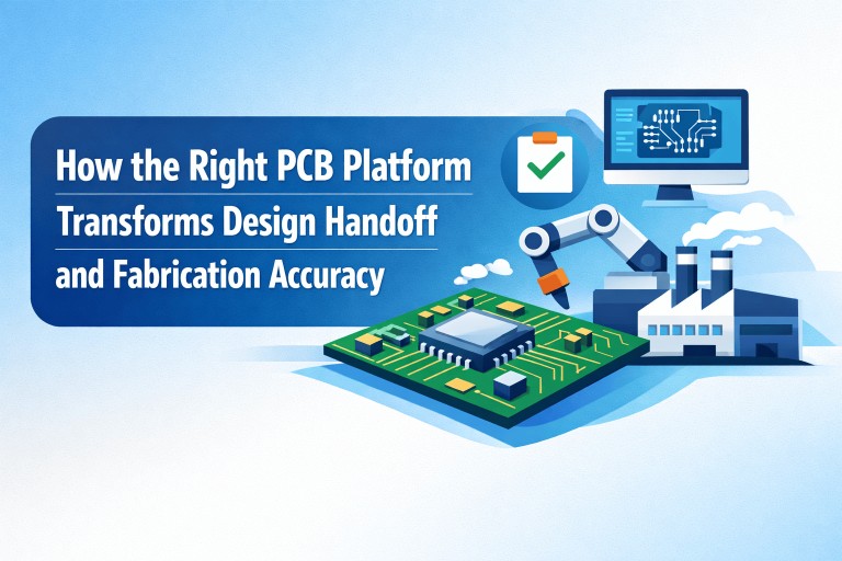
The Role of a Robust PCB Platform
A robust PCB platform serves as the backbone for all subsequent activities, from schematic capture to final fabrication data extraction. It provides a unified workspace where designers can manage signals, power distribution, and component placement without switching between disparate tools. This cohesion reduces the likelihood of misinterpretation or data loss that often occurs when files are manually transferred between separate applications. Moreover, a platform that incorporates industry‑standard design rules automatically flags potential issues, allowing engineers to address constraints early. Such proactive error detection is especially valuable in high‑density or high‑speed designs where even a minor routing mistake can lead to significant performance degradation.
Streamlining Design Handoff
One of the most critical stages in the PCB development cycle is the handoff from design to manufacturing. A seamless handoff requires accurate, complete, and well‑organized data, and the platform must facilitate the generation of all necessary files—Gerber, drill, BOM, and assembly drawings—in a single, repeatable workflow. By embedding these capabilities into the design environment, engineers eliminate the need for manual file conversion, which is a common source of errors. The platform’s ability to maintain a single source of truth ensures that the same design is reflected in every output, providing manufacturers with confidence that the board will meet specifications without unexpected surprises.
Ensuring Fabrication Accuracy
Fabrication accuracy hinges on the precision of the data supplied to the PCB manufacturer. Advanced platforms enable designers to define exact layer stackups, copper weights, and trace widths with millimeter‑level precision. Automated DRC (Design Rule Check) engines cross‑verify these parameters against manufacturer capabilities, flagging any conflicts before the board goes to production. Additionally, the integration of 3D modeling tools allows designers to visualize component placement and verify clearance requirements in real time. This level of detail reduces the risk of mechanical interference, signal integrity issues, and costly rework cycles, ultimately leading to boards that perform as intended from the first test.
Data Integrity and Version Control
Maintaining data integrity across a project’s lifecycle is essential, especially when multiple engineers collaborate on the same design. A robust platform offers built‑in version control, allowing teams to track changes, revert to previous states, and document decision rationales. This audit trail is invaluable when troubleshooting issues or when the board must be re‑fabricated due to a design change. By centralizing all files and maintaining a strict change history, the platform minimizes the risk of orphaned or conflicting data that can derail a project. In environments where regulatory compliance is required, such traceability becomes not just a convenience but a necessity.
Collaboration Across Teams
Modern PCB projects often involve cross‑functional teams spanning design, manufacturing, and quality assurance. A platform that supports real‑time collaboration, such as shared project workspaces, streamlines communication and reduces turnaround times. Engineers can annotate designs, share feedback, and resolve conflicts without leaving the environment. This transparency fosters a culture of continuous improvement and ensures that every stakeholder has visibility into the board’s status. When design changes are made, the platform can automatically propagate updates across all relevant documents, keeping the BOM, schematics, and layout in sync and preventing miscommunication.
Cost and Time Savings
Every hour spent on debugging or re‑fabricating a board translates into direct financial losses. By catching design errors early and ensuring that manufacturing data is flawless, a capable PCB platform cuts both time and cost. Automated rule checks reduce the need for manual reviews, while integrated simulation tools help validate electrical performance before a prototype is built. These efficiencies accelerate the time‑to‑market, giving companies a competitive edge. Additionally, fewer revisions mean lower material and labor costs, which can be passed on to customers or reinvested in product development.
Real-World Case Studies
Consider a consumer electronics company that transitioned from a fragmented design workflow to a unified platform. Within the first quarter, they reduced board rework by 35% and cut prototype build time from 12 to 6 days. Another example comes from a medical device manufacturer that leveraged the platform’s EM simulation capabilities to meet stringent EMI compliance, avoiding costly redesigns. These case studies illustrate that the right PCB platform is not merely a tool but a strategic asset that can transform product quality and delivery performance.
Choosing the Right Tool for Your Workflow
Selecting an appropriate PCB platform involves evaluating several factors: the complexity of the designs, the size of the engineering team, integration with existing CAD tools, and the level of support required for manufacturing partners. It is also crucial to assess the platform’s scalability—whether it can handle the increasing number of layers, finer pitch components, and higher frequency signals that future products may demand. By aligning the platform’s capabilities with the organization’s long‑term goals, companies can future‑proof their design process and avoid costly migrations.
Conclusion
In the fast‑paced world of electronic design, the right PCB platform is a catalyst for innovation and reliability. It streamlines the handoff process, enforces fabrication accuracy, and supports seamless collaboration, all while safeguarding data integrity. By investing in a platform that meets these criteria, companies position themselves to deliver high‑performance boards faster and more cost‑effectively. For teams looking to elevate their design workflow, exploring solutions such as the Allegro PCB can unlock new levels of precision and efficiency, ensuring that every board that leaves the workshop is built to exacting standards.